5. VERILOG TUTORIAL 1 : CIRCUIT DESIGN WITH VERILOG
In this tutorial, we will not explain all of Verilog, but just the bare minimum which is relevant for this course. This means we will cover a tiny subset of the total Verilog specification..
5.1 What is Verilog?
Before we start explaining Verilog in some detail, it may be a good idea to get a bird's eye view of of what it does, and how it is different from other high-level languages like C or Python..
Let us first remember why we use C when we program a computer: After all, we can write our program in machine language also. And, machine language is the only language that is understood by a CPU, hence even if we write everything in C it should be converted into machine code before being run on a CPU. So, why bother with C?
Actually, at this stage in our lives as computer engineers, we all know the answer: Writing, changing and maintaining even tiny programs directly in machine language is extremely hard for us, humans. It is only for this reason that we opt for writing our programs in C, and then use a C compiler to convert them into machine language..
C program ---> C compiler ---> Machine language ---> Run --> Program works and prints out the results
In other words, C or any other high-level language only exists for our sake. By using a high-level language we can describe what we want the computer to do without going into the machine-language details of the particular computer on which our program will run. The CPU in our computer, for its part, neither understands nor needs a high level language. All it needs is something written in machine code.
Verilog serves a similar purpose. When we want to design some hardware, we need to produce a circuit diagram which describes it gate-by gate. Our first step is generally to take pen and paper and draw such a circuit diagram in terms of its basic elements, like gates, multiplexers, registers etc. But this is very similar to programming in machine language. Modern hardware is too complicated to be drawn on paper. What is needed is a high-level language which is powerful enough to be used to describe how a hardware circuit behaves. We just want to use such a high level language to describe what we want our circuit to do, and how we want it it to behave under various circumstances. And then use a compiler to compile it and produce the gate-by-gate schematic. Verilog is one such high-level language.
After we describe our circuit in Verilog, we compile it with a Verilog compiler.. As a C compiler translates our C program into machine language, so does a Verilog compiler expands our Verilog program into a circuit schematic with very low level of detail.
High level circuit description,
written in Verilog              ---> Verilog compiler ---> Low level Circuit schematic
                                                               (a .blif file)
Of course, when we say "circuit schematic", we don't mean that Verilog compiler generates a stack of papers with some schematics on it. It instead generates a file indicating how many flip-flops, gates, multiplexers etc. must be used, and how they must be connected to each other to realize the desired hardware. Generally, open source Velilog compilers like Odin-II use .blif file format for such a description. In closed source Verilog compilers like Quartus this information is a commercial secret.
A serious mistake usually committed by students who learn Verilog is the unfounded assumption that Verilog programs is written to be "run", just like other programming languages. Verilog programs are not "run" after being compiled. Instead, the .blif file they generate is used to build a circuit.
5.2 Verilog Constants and Variables
5.2.1 Constants
In Verilog, when we write down a constant, we have to specify how many bits it takes, and what is the base we use to represent it. A few examples are
- 5'b10010 5 bit binary number 10010
- 12'b101 12 bir binary number 000000000101.
- -7'b101 twos complement negative of 7-bit binary number 101, ie,
- 11'hf7a the rightmost 11 bits of the hexadecimal number f7a, ie, 77a.
- -11h'27a twos complement negative
5.2.2 Variables
There are two different types of Verilog variables
- wire variables
- reg variables
When Verilog is first designed, wire variables are intended to hold combinatorial results, while reg variables are intended to hold sequential results. Today this distinction is largely surpassed. While wire variables are still limited to combinatorial results only, reg variables are expanded in scope and now they can hold both combinatorial and sequential results. The exact nature of the difference between the wire and reg variables will be discussed further below..
Simple Verilog variables (wire or reg) are binary, ie, they can only be set to 0 and 1 and no other value. When a variable is desired to represent more than one bits, it is declared as an array. Below are a few examples of declaration:
- wire x //x is a one bit wire variable
- wire [3:0] conn //conn is a 4 bit wire variable
- reg y // y is a one bit reg variable
- reg [11:0] abc //abc is a 12 bit reg variable
Array elements and subranges work in the usual way. If we continue from the above examples
- comm[2] refers to the second element of comm
- abc [5:3] refers to the subrange of bits 5,4,3 of abc.
- abc refers to the 12-bit reg variable abc.
It is also possible to have two dimensional arrays. An example declarations are
reg[15:0] mem [0:512]; // 1KByte memory of 16-bit words.
The usage is as follows:
- mem[47] // 47th location in the variable mem. An 16-bit variable..
- mem[5][65] // 5th bit of 65th location in mem.
- mem[5:3][114] //subrange of bits 5, 4, 3 of 114th location in mem.
Higher dimensional arrays are also possible but in this lecture we will not need them..
5.3 Verilog Modules
A complete hardware circuit must have
- Input ports
- Output ports
- Some logic to receive inputs and generate outputs
Such a circuit is described by a "module" in Verilog, which has the following format:
module module_name(input and output ports)
declaration of input ports;
declaration of output ports;

declaration of local variables;
statements to describe the logic
endmodule
Modules in Verilog are analogs of functions/procedures in other programming languages. As can be seen from the above format, they contain
- Keyword module, followed by module name and a list of module's input/output ports
- Input and output port declarations
- Local variable declarations
- Statements that describe the internal logic of the circuitry, which is composed of four categories: Combinatorial or sequential always blocks, assign statements and calls to other modules.
- Keyword endmodule.
Below, we will investigate each of these elements.
Note that a module can call other modules. A Verilog project is nothing but a hierarchical collection of interlinked modules, with the top module representing the project.
5.4 I/O Port and Variable Declarations in a module
Verilog modules contain three different sort of variables:
- Input variables (Also called input ports)
- Output variables (Also called output ports)
- Local variables
Input variables can only be declared as wire type. Output variables can be both wire and reg types. It is not necessary to use keyword "wire" when declaring a wire type input or output variable. Keyword "reg" must be used when a reg type output variable is declared.
Verilog modules use input and output ports to receive/send data from/to outside, and use local variables for local computation. Let us give an example:
module foo(x,y,count,a,b)  //module foo has 5 ports
input [4:0] x, count       //x and count are 5 bit input ports.
input y                    //y is a 1-bit input port.
output [2:0] a             //a is a 3-bit wire type output port
output reg [1:0] b;        //b is a 2-bit reg type output port

reg [3:0] aa, loc1         //aa and loc1 are 4 bit reg type local variables
wire [1:0] cc              //cc is a 2-bit wire type local variable.


          ... statements ...

endmodule
5.5 Combinatorial circuit design in verilog
We have learned that digital circuits can be roughly classified into two groups: Combinatorial and sequential. Let us first remember in what ways these two differ..
5.5.1 Combinatorial Circuits 1 : Basic Design
Consider a combinatorial circuit with three 1-bit inputs (a, b, c) and two 1.bit outputs (x, y):
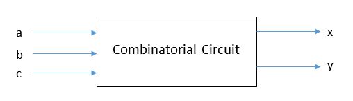
As soon as any of the inputs a, b, c change, the outputs x, y will also change.. In all combinatorial circuits, there is a very small propagation delay between inputs and outputs. How small? Much smaller than the clock period. Other than that, we can say that outputs follow inputs instantaneously. Actually, a combinatorial circuit is equivalent to a truth table and it is completely independent of the clock.
A combinatorial circuit can be defined in two different ways in Verilog:
- "Combinatorial" always blocks
- Assign statements
We will start with assign statements, which is the simpler of the two.
5.5.1 Assign Statements
Suppose that we want to write a Verilog module that realize the following combinatorial circuit in Verilog:
5.5.2 Combinatorial Always Blocks
Let us list the salient properties of combinatorial always blocks:
Combinatorial always blocks start with the keyword "always_comb"
The keyword always_comb is followed by a begin...end block.
The code within the begin...end block describes the circuit.
That code consists of three different kinds of statements: blocking assignment statements, if statements and switch statements..
Let us write down some example modules whose body consist of combinatorial always blocks:
Example 1:
Assume that we have the following module:
module foo1(a,b,c,y)
input a, b, c;  //three one-bit variables as inputs
output reg y;   //a single one-bit variable as output.
reg x;          //a one-bit local variable

always_comb
begin
   x = (a | b) & c   //blocking assignment
   y = x & c         //blocking assignment
end
endmodule
will generate the following circuit:
========> FIGURE HERE
Blocking assignment statements.
Note that all the operations are the same with C (ie, | denote OR, & denote AND etc)
In the generated circuit, if any variable on the RHS (ie, a,b,c,x) changes, the LHS's (ie, the variables x and y) will also change instantaneously.
You shouldn't perceive this code as you perceive a C or Python code. A Verilog code is not written to run "line by line" as them. Instead, a verilog code is written to generate a circuit. Therefore, only the connectivity information encoded in the program is important, ie, a, b and c connect to x, and x and c connect to y. Hence, unlike C or Python, the ordering of the lines within a module is unimportant. The combinatorial always block in the above program can also be written as
always_comb
   y = x & c
   x = (a | b) & c
end
This writing is also correct and will generate exactly the same circuit, even though varable x is "used" (in line 2) before it is "assigned a value" (in line 3). Even more curiously, we can divide this always block into two always blocks, and the code will still be correct
always_comb
   y = x & c

always_comb
   x = (a | b) & c
The ordering of always blocks is also unimportant. Note that we do not need "begin" and "end" keywords when an always block contains only a single assignment.
Example 2:
The module
module foo2(in1, in2, add, msb)
output reg [3:0] add
input [3:0] in1, in2
output reg msb
reg [3:0] sub       //local variable

always_comb
begin
   msb = add[3] & sub[3]
   add = in1 + in2
   sub = in1 - 4'h7
end
endmodule
will generate the following circuit:
========> FIGURE HERE
Even this diagram is high level. We have used a 4-bit adder block and a 4-bit subtractor block in order not to clutter the figure. The circuit generated by Verilog will replace these blocks with circuits formed from elementary logic gates. Except, in some cases, the FPGA this circuit will be loaded on contains ready-made adders. In such cases, Verilog will utilize these.
The most important advantage of the combinatorial always blocks in comparison to the assign statement is that it can use block structure.
5.5.4 If statement in combinatorial always blocks
"If" statements in Verilog are used to construct multiplexer-like circuits. Consider the following module
module foo1(a,b,res)
input [3:0] a, b;
output reg [3:0] res;
input operation;

always_comb
if (operation=1b'1) \\as this if..else construct constitute a single statement, we
    res=a+b;        \\dont need begin..end keywords in the always block.
else
    res=a-b;
endmodule
This generates the following circuit
===========> figure
Multiplexer networks can also be constructed via if-elseif-else statements. For example, the following code
module foo1(a,b,c,res)
input [3:0] a, b;
output reg [3:0] reg;
input [1:0] operation;

always_comb
if (operation=2h'0) \\as this if..else construct constitute a single statement, we
    res=a+b;        \\dont need begin..end keywords in the always block.
else if (operation=2h'1)
    res=a-b;
else               \\operation=2h'2 or operation=2'h3
    res=b;
endmodule
generates this circuit
=============> figure
Each if, elseif and else construct generates a multiplexer in the multiplexer chain.
If statements can be nested, and much more complicated circuits can be formed. For example
reg f, g;
always_comb
  if (sel == 1)
    begin
      f = a;
      if (sel_2 == 1)
        g = ~a;
      else
        g = ~b;
    end
  else
    begin
      f = b;
      if (sel_2 == 1)
        g = a & b;
      else
        g = a | b;
    end
This will generate the circuit in the following figure:
=========> figure
Note that there is a multiplexer chain for each of the two variables (f and g) assigned.
5.5.5 case statement in combinatorial always blocks
Case statements, like if statements, is used to construct multiplexer circuits. For example, the code
module foo1(a,b,c,res)
input [3:0] a, b;
output reg [3:0] reg;
input operation;

case (a)
    1b'1 :  res=a+b;
    1'b0 :  res=a-b;
endcase

endmodule
This will generate the same circuit as in figure .. Consider the more complicated code
module foo1(a,b,c,res)
input [3:0] a, b;
output reg [3:0] reg;
input [1:0] op;

always_comb
case (op)
    2'h0 : res=a+b;
    2h'1 : res=a-b;
    default : res=a; \\handles all the remaining cases, ie, when op=2h'2 or op=2'h3
    res=b;
endmodule
This code is functionally the same with the above example, but it will generate a different circuit
========>
Generally, if-elseif-else structures tend to use a multiplexer chain with many small multiplexers. This uses a small number of gates to synthesise, but signal propagation through such a network is slow. On the other hand, case statement use one big multiplexer.. This approach uses a lot more gates, but signal propagation is fast.
if-elseif-and statements and case statements can be used in a nested way. For example:
always_comb
case (sel)
1'b1: begin
      f = a;
      if (sel_2 == 1)
        g = ~a;
      else
        g = ~b;
      end
1'b0  begin
      f = b;
      if (sel_2 == 1)
        g = a & b;
      else
        g = a | b;
      end
endcase
5.5.6 Incomplete assignment problem and inferred latches
When we create a combinatorial circuit, we are basically creating a truth table. In a truth table (or, in a combinatorial circuit which realizes it), there is no memory. For each possible input, there should always be a well-defined output. Recall that this is not so in sequential circuits. They may generate different outputs for the same input, depending on their memory state.
Assume that we want to realize a combinatorial circuit with the following truth table:
5.6 Sequential Design
Contrast the combinatorial circuit described above with the sequential circuit given below, which also has three inputs (a, b, c) and two outputs (x, y):
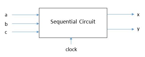
Note that in sequential circuits, in addition to the usual inputs and outputs, we have a clock input, which will play an immensely important role. The outputs will only be updated by the inputs at the clock edges. At all other times, the outputs just remember the previous inputs and do not change. We will also have a load input, as we will use a register instead of a flip-flop as a memory element. At the clock edges, the outputs will be updated only when load=1.
There is only one way to define a sequential circuit in Verilog: A sequential always block.
A Verilog program is a large module (circuit), which contains other modules (subcircuits) within it. Each module is formed from always blocks, assign statements, and other, smaller modules.
5.7 Module Hierarchy
Below is a two-bit equality tester module:
Module eq1(i0,i1,eq)
input wire i0, i1;
output wire eq;

wire p0, p1;
assign eq = p0 | p1;
assign p0 = ~i0 &~i1;
assign p1 = i0 & i1;
endmodule
To construct a two-bit equality tester, we may invoke 1-bit equality tester module two times.
module eq2(
(
input wire [1:0] a,b;
output wire aeqb;
)
wire e0, e1;
eq1 eq_bit0( .i0(a[0], .i1(b[0]), .eq(e0) )
eq1 eq_bit1( .i0(a[1], .i1(b[1]), .eq(e1) )
assign aeqb = e0&e1;
endmodule
Nested modules are not allowed in Verilog (but they are allowed in SystemVerilog).